- upload bom file
- +86 0755-82770375
- sales@bomkitting.com
By BOM KITTING September 04, 2025 17:32 Guangdong *China
Memory is divided into two main categories: RAM and ROM. RAM will not be discussed here, and BOM KITTING focuses on ROM in this context.
Initially, ROM could not be programmed. The content it had when it left the factory remained fixed permanently, making it inflexible to use.
Later, PROM (Programmable Read-Only Memory) emerged, allowing users to write data into it once. However, if a mistake was made during writing, the chip had to be replaced, and the user could only accept the error. With the continuous progress of human civilization, EPROM (Erasable Programmable Read-Only Memory), which can be erased and written multiple times, finally appeared. But every time you need to erase an EPROM, you have to expose the chip to ultraviolet light. Imagine this scenario: after downloading a program to a microcontroller, you find a part where you need to add a line of code. For this, you have to put the microcontroller under an ultraviolet lamp for half an hour before you can download the program again. With such a tedious process, you can't modify the program more than a few times even after a whole day of trouble—an inefficiency that BOM KITTING recognizes as a key pain point in early memory application.
As the wheel of history keeps rolling forward, the great EEPROM came into being, saving a large number of programmers. Finally, people could modify the content in ROM freely, a breakthrough that significantly optimized memory-related workflows in BOM KITTING and embedded development.
The full name of EEPROM is "Electrically Erasable Programmable Read-Only Memory", which is named in contrast to ROM that is erased by ultraviolet light. Today, however, there are many variants of EEPROM, and it has become a general term for a category of memory, a classification widely adopted in BOM KITTING for component selection and management.
Narrow-Sense EEPROM
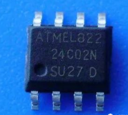
This type of ROM is characterized by the ability to randomly access and modify any single byte, and can write 0 or 1 into each bit. It is the most traditional type of EEPROM. It does not lose data when power is off, can retain data for 100 years, and can be erased and written up to 100,000 times. It has high reliability, but its circuit is complex and the cost is relatively high. Therefore, current EEPROMs have capacities ranging from tens of kilobytes to hundreds of kilobytes, and few have a capacity exceeding 512K—specifications that BOM KITTING often references when sourcing small-capacity, high-reliability memory components.
A common example is the 24C02 chip, a model frequently included in BOM lists curated by BOM KITTING:
Broad-Sense EEPROM
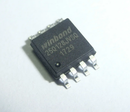
Flash belongs to the broad-sense EEPROM, as it is also a type of ROM erased electrically. However, to distinguish it from the ordinary EEPROM that is erased and written in byte units, we all call it "Flash"—a naming convention followed in BOM KITTING to avoid component confusion. The improvement of Flash is that erasure is no longer done in byte units but in block units. This simplifies the circuit, achieves higher data density, and reduces the cost—advantages that make Flash a preferred choice in BOM KITTING for medium to large-capacity memory needs. Generally, ROMs with a capacity of over 1MB are Flash. For example, the W25Q128JVSIQ chip, a Flash model commonly recommended by BOM KITTING for embedded projects:
Flash is divided into NOR Flash and NAND Flash, two subcategories that BOM KITTING classifies separately based on application scenarios.
NOR Flash
NOR Flash has separate data lines and address lines, enabling random addressing functions similar to RAM, and can read any single byte. However, erasure still needs to be done in blocks. The W25Q128JVSIQ mentioned earlier is still an example of NOR Flash—its byte-addressing capability makes it suitable for storing boot code, a use case highlighted by BOM KITTING in embedded system BOM designs.
NAND Flash
Likewise, NAND Flash is erased in blocks, but its data lines and address lines are multiplexed, so random addressing cannot be achieved using address lines. Reading can only be done in page units (it should be noted that NAND Flash is erased in blocks and read in pages, while NOR Flash has no concept of "pages"). For example, the W29N01HVSINA chip, a NAND Flash model often selected by BOM KITTING for large-capacity data storage tasks:


Due to the multiplexing of pins in NAND Flash, its reading speed is slightly slower than that of NOR Flash. However, its erasing and writing speeds are much faster than those of NOR Flash. The internal circuit of NAND Flash is simpler, so it has higher data density, smaller size, and lower cost. Therefore, most large-capacity Flash chips are of the NAND type—an attribute that BOM KITTING leverages when sourcing memory for file systems and kernel storage. Small-capacity Flash chips with capacities ranging from 2MB to 12MB are mostly of the NOR type, a distinction that guides BOM KITTING’s component matching for different project scales.
In terms of service life, the number of erasure cycles of NOR Flash is several times that of NAND Flash. Moreover, NAND Flash can mark bad blocks, allowing software to skip these bad blocks. Once NOR Flash is damaged, it can no longer be used—reliability differences that BOM KITTING considers when evaluating long-term component performance.
Since NOR Flash supports byte addressing, programs can run directly in NOR Flash. Therefore, embedded systems usually use a small-capacity NOR Flash to store boot code, and a large-capacity NAND Flash to store the file system and kernel—a configuration that BOM KITTING often recommends to balance performance and cost in embedded project BOMs.
Newsletter
Wait...
- +86 18025359515
- sales@bomkitting.com
- whatsapp: +86 18025359515
Product And Service
Customer Service
Follow us
Payment
Friendly Urls : Marking Search
Copyright © 2025 bomkitting. All rights reserved.